Not all pixels are created equal, however. For this reason, manufacturers of display devices have turned from LCD (liquid crystal display) technology toward new OLED (organic light-emitting diode), miniLED, and microLED technologies. This shift has provided consumers with improved visual experiences but has added production challenges for display manufacturers.
Pixel illumination methods are at the root of the trend. LCD pixels do not produce their own light. Instead, these displays use transmissive methods, illuminating their pixels from behind using a backlight unit, or BLU, comprised of LEDs. Because LCD pixels rely on a uniform light source for illumination, it is not easy to adjust light emitted through each pixel. The result is limited contrast between light and dark areas of the display because “black” pixels still receive some amount of light from neighboring areas of the illuminated display.
This is not a problem for OLED, miniLED, and microLED displays. These technologies are emissive, meaning they have self-illuminating pixels. Driven independently to emit their own light, these pixels can be independently adjusted or completely turned off, providing absolute blacks for dark areas of the display – even when neighboring pixels are illuminated.
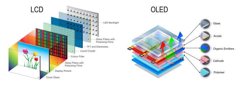 Above: Left: Layers of a transmissive LCD with uniform LED backlight, which illuminates display pixels from behind. Right: Layers of an emissive OLED display and subpixel emitters, each producing its own light.
While the absence of a unifying backlight is beneficial for contrast, it makes emissive display uniformity difficult to control. Each pixel responds differently to different driving conditions (electrical current) and may appear brighter or dimmer than its neighbors. Color is similarly impacted. Each pixel in a display is made up of red, green, and blue subpixel elements. In emissive displays, subpixels are also independently emissive, with different brightness levels causing variations in color that impact overall display appearance. If nonuniformity (called “mura” – Japanese for “unevenness”) is not controlled during the production process, the result is poor visual quality that can impact production efficiency and brand perception.
Automated visual inspection systems provide quality control for display production. Imaging colorimeters are especially useful for evaluating displays because they apply specialized color filters and calibrations to measure values of brightness (luminance) and color (chromaticity) according to standard human visual response (i.e., measuring displays as they are seen by a user). These systems also measure entire displays in a single image, enabling quick comparison of values across the display area to detect issues like mura.
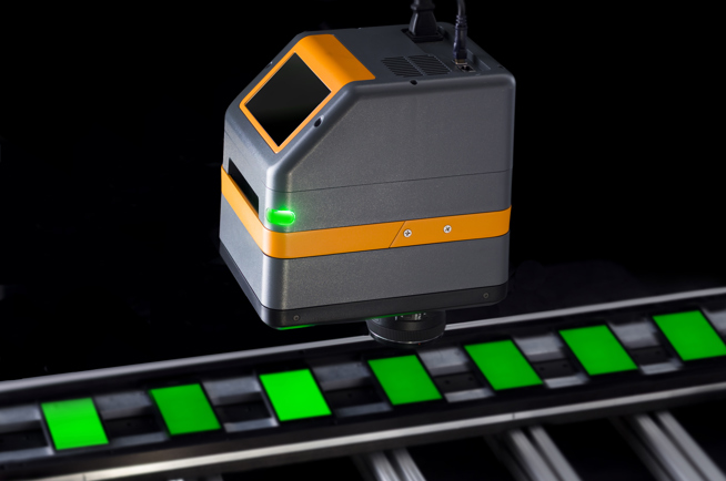 Above: An imaging colorimeter evaluates the visual appearance of displays in production. Shown: Radiant Vision Systems ProMetric Imaging Colorimeter.
For emissive displays, mura is determined at the pixel level. Imaging colorimeters must quantify brightness and color within the area of each emissive element to detect defects. Pixel-level measurement also allows discrepancies between pixel and subpixel output to be calculated as objective values. With these values known, manufacturers can adjust driving conditions for each pixel, thereby correcting pixel output to produce uniform brightness and color across the display.
Pixel uniformity correction is called “demura” because it eliminates mura from the display. Demura methods ensure quality products and reduce waste of costly display components that have poor (but correctable) performance. Consider microLEDs, where manufacturing costs are high and producing a single display is difficult – the more a manufacturer can do to eliminate potential issues in display performance, the more they can improve their bottom line. Often, demura is applied at several stages throughout device manufacture to catch issues early and often.
Just as no two pixels are exactly alike, however, demura solutions (equipment, solution providers, and techniques) vary in their efficacy for correcting displays. Accurate measurement is critical – but it is extremely challenging to capture luminance and chromaticity values within a region as small as a single subpixel. As display resolutions increase and pixels shrink and become closer in proximity, they become harder for imaging systems to isolate for measurement. The risk is “garbage in, garbage out” – if an inaccurate measurement is made, an inaccurate correction will be applied. Ultimately, a “corrected” display could look worse than the original uncorrected display.
A viable demura method employs a high-resolution imaging colorimeter (typically 29 megapixels and above) to measure all display pixels in a single image. Single-image measurement increases cycle times for production operations. Higher imaging resolution is needed to apply more sensor pixels (discrete photo-sensing elements on the imaging system’s CMOS or CCD image sensor) across each display pixel to ensure sufficient detail for isolation and measurement. As display resolutions increase relative to imaging resolutions, however, most image-based measurement systems can only apply a few (less than 10) sensor pixels across each display pixel in a single measurement image. Demura, therefore, often relies on image processing and analysis techniques to improve imaging precision to better isolate and capture pixel output values using limited sensor-pixel information.
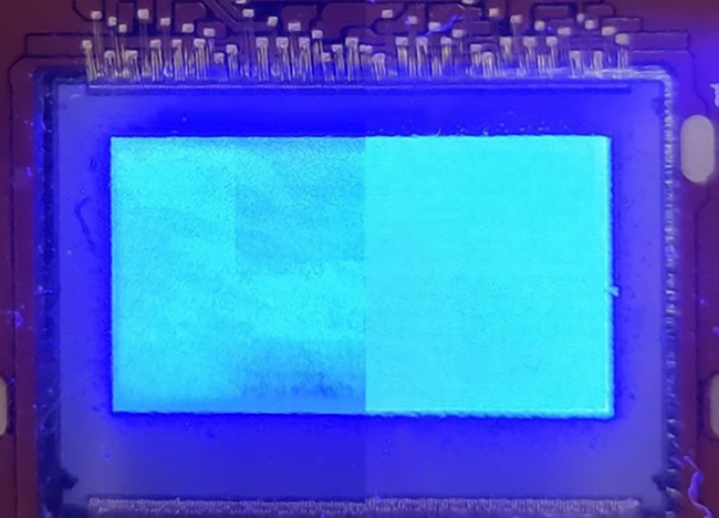 Above: Actual results of demura applied to a microLED microdisplay, utilizing pixel-level measurements captured by a Radiant Vision Systems ProMetric I29 Imaging Colorimeter.
For example, a “fractional pixel” measurement method patented by Radiant Vision Systems (US Patent 10,971,044) uses luminance values to hone in on display pixels. Based on the highest luminance values measured in an image, a measurement region (region of interest) is drawn around the area of each pixel. With the bounds of the pixel defined, the factional pixel method then improves measurement by factoring only the values captured by fractional areas of the sensor pixels that fall within the region of interest. These values are aggregated to provide the measurement of a single display pixel. This is done without factoring in values from neighboring pixels that cross into the same sensor pixels applied to the target display pixel. In studies,1 the fractional pixel method has been shown to reduce errors in pixel-level measurement over traditional methods as much as 80%.
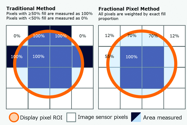 Above: Fractional pixel measurement method (US Patent 10,971,044; assignee: Radiant Vision Systems LLC) measures the exact area of image sensor pixels within the region of interest defined for a single display pixel.
Emissive displays will continue to demand visual inspection that can extract actionable data from measurement areas as small as today’s shrinking display pixel. As pixels become smaller and more diverse in their characteristics, display manufacturers rely on the innovation of measurement experts to ensure pixel-perfect devices and efficient production operations. Effective demura is one small but powerful part of display innovation that drives quality, efficiency, and viability of new display technologies for consumers and new applications.
Reference:
1. Pedeville, G, Rouse, J, and Kreysar, D, “Fractional Pixel Method for Improved Pixel-Level Measurement and Correction (Demura) of High-Resolution Displays,” Society for Information Display (SID) Display Week 2020 Digest, Book 2, August 2020.
Find out more: A look at measuring microLEDs for pixel uniformity correction.