
The discovery of novel function materials is vital in the development of technologies that can transform consumer experiences and boost sustainability, such as solar cells, more efficient batteries and transparent electronics. Yet there is currently restricted analysis of these materials in order to identify their specific configuration – in contrast to the advancements now being fueled by AI in discovering material from chemical formulations.
This constraint is the result of a lack of appropriate tools to help speed up the analysis process. To solve this, researchers at the US Massachusetts Institute of Technology (MIT) have created an innovative high-throughput analysis method that leverages computer vision, to determine the band gap and stability of newly synthesized semiconductor materials.
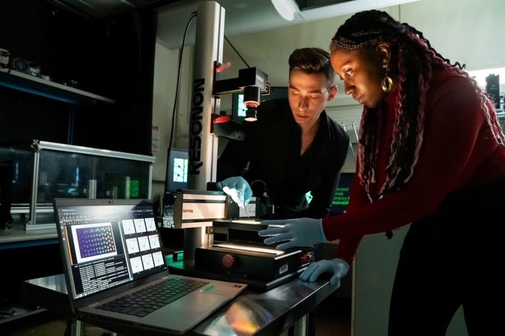
The MIT research team included graduate students Alexander (Aleks) Siemenn and Eunice Aissi, alongside graduate student Fang Sheng, post doctorate Basita Das, and professor of mechanical engineering Tonio Buonassisi, former visiting professor Hamide Kavak of Cukurova University (Turkey) and visiting post doctorate Armi Tiihonen of Aalto University in Finland. Together, they set out to develop a set of automated characterization (autocharacterization) algorithms to accelerate the measurement of material properties important for understanding the performance of semiconductor materials. And the team found that their selected algorithm tools substantially improved the analysis and assessment of newly integrated electronics materials.
The MIT scientists developed their algorithms using a combination of computer vision and image processing techniques, that enabled the rapid parallel processing of many materials in an automated fashion. Previously, the characterization of electronic material properties, such as band gap and stability, was a slow and manual process requiring a domain expert. As research team member, Aleks Siemenn, explains: “Conventional techniques were creating a bottleneck in the pipeline of high-performance semiconductor materials discovery. Our research objective was to alleviate the characterization tailback by developing fast and automated methods of quantifying these important properties of semiconductors and electronic materials.”
Crucial testing regimes
As ever, testing regimes were integral to the rigor of this research. In order to generate concrete results, the study team’s algorithms passed through a series of stage gates during testing, to validate tools and ensure high accuracy. Explaining the process, MIT team member, Eunice Aissi, says: “Typically, this begins with testing the code on dummy datasets to work out bugs. Then, we proceed to the analysis of simple materials and crosscheck our output with known values published in literature.” Lastly, the MIT team moved to testing across more complex materials for validation. Using this developed hierarchical testing regime, they calculate that they achieved accuracies of over 96% on both of their autocharacterization algorithms.
The ultimate goal with these algorithms is to engineer tools robust enough to perform accurate material property quantification, even when run on novel materials that have not previously existed. The researchers’ autocharacterization tools autonomously compute the band gap and stability of compositions. The band gap of an electronic material is significant as it determines whether the material is a conductor, semiconductor or insulator. Materials with small band gaps have easily moving electrons which results in high conductivity; and materials with larger band gaps have a limited number of available energy levels for electrons, generating lower electrical conductivity.
The first algorithm implemented by the MIT team is designed to process visual data from detailed, hyperspectral images. A hyperspectral image has 300 channels which the algorithm transforms to rapidly calculate the specific band gap. In addition, stability refers to a material’s ability to maintain its structure and characteristics under various conditions, such as temperature or pressure change. It is imperative to confirm the stability of newly synthesized materials to ensure they perform robustly in electronic applications that include photovoltaic systems or solar cells.
The second algorithm used by the team analyses standard RGB (red, green and blue) images and assesses a material’s stability based on visual changes in the material’s color as they occur. The researchers found that this color change helped to identify the degradation rate of the material being studied.
There are many key features that can be extracted from optical data of electronic materials, such as semiconductors, if the data resolution is high enough. Identification of the surface uniformity of a material or the degradation of a material over time can also contribute to electronic material evolution. According to Aleks Siemenn, the study utilized: “High-resolution hyperspectral imaging, capable of capturing the intensities of hundreds of wavelengths of light within a single pixel.” This works in tandem with computer vision to compute the band gap of semiconductors. As Siemenn explains: “Similarly, we utilize computer vision parallel processing of highly resolved temporal images of semiconductors to measure their rates of degradation, otherwise known as stability.”
Overcoming obstacles
The study was not without its challenges, as the team needed to deal with rapidly processing large volumes of high-resolution data in an efficient manner. Since a key aim of their chosen tools was to minimize the time it takes to perform characterization of materials, the algorithm compute time was critical.
In fact, implementing rapid data processing techniques, such as date vectorization which runs many computations in parallel rather than one at a time, enabled the team to speed up the efficient nature of complex data processing to identify and characterize around 70 printed semiconductor samples.
Industry benefits
For consumer electronics companies, there are a multitude of advantages to be gained from this research. The widespread implementation of automated synthesis and characterization techniques means that the speed and reliability of new materials discovery can be increased.
With the tools developed in this study, MIT specifically targeted the discovery and optimization of new, high-performance semiconductor materials. Further development of these tools may also extend their applicability to improving the performance of other types of electronic materials, including flexible and transparent electronics, LEDs, and solar panels. Looking ahead, Siemenn says: “One of our main goals for the future development of these autocharacterization algorithms is to extend their application to many different material compositions without sacrificing their evaluation speed or accuracy.”
Future work
In the quest for valuable synthesized materials, researchers worldwide are developing ‘labs of the future’, where AI-steered robots are helping to accelerate new discoveries. An A-Lab (autonomous lab of the future) facilitates the work that scientists, such as the MIT team, are evolving in the area of composition computation.
Summing up the future aims of their A-Lab, Eunice Aissi comments: “The goal of this lab is to make and measure thousands of materials per day to aid in the discovery of novel, high-performance functional materials utilizing the tools we have developed in conjunction with robotics and machine learning methods.”
• The MIT team has published details of its research in the journal Nature Communications (https://www.nature.com/articles/s41467-024-48768-2).