
Photonics – which encompasses the study of light generation, modulation, processing, amplification, detection and more – has increasingly become a focal point of technological advancements in the consumer electronics industry. Photonics is based on the use of photons to transmit data, in contrast to conventional electronics which relies on electrons for transmission. And this fundamental difference gives photonics a number of advantages, including greater speed, bandwidth, and versatility.
Over the past few decades, photonics has transitioned from a largely theoretical field into a cornerstone of many modern applications. It has silently revolutionized countless aspects of our lives – for example, in the form of fibre optic cables, which serve as the basis of today’s global telecommunications by using light to transmit data over long distances with minimal loss. More and more, however, photonics is being integrated directly into consumer-facing devices and objects that we use every day.
Displays, including televisions, monitors, phone screens, AR and VR headsets, and more, feature higher resolutions, improved color accuracy, and faster response times thanks to photonic principles. Flexible and foldable screens also owe their existence to photonics. Cameras can use photonic technology to capture light more effectively, and incorporate sensors that measure the distance between lenses and other objects, enhancing features like portrait mode, facial recognition, and AR applications. In wearables, photonics is responsible for optical heart rate monitoring and pulse oximetry, integrated solar charging, optically driven wireless connections, and more.
Photonic components can also be found in many smart home devices, automotive and healthcare applications, and even environmental management systems, where photonic sensors can be used to detect pollutants and measure real-time air quality.
Lighting the way
Dr Martin Virte, Professor of Photonics at Vrije Universiteit Brussel (VUB), says it is unlikely that the field of photonics will ever replace that of electronics. Instead, he predicts, we will see the two fields become increasingly integrated, with each helping to overcome the limitations of the other.
Artificial intelligence and quantum computing are two major areas where this will most likely occur. Meeting the high-frequency data processing demands of AI and the precision required for quantum transmissions will unlock new frontiers of connectivity, not only in terms of speed but also proximity and distribution, laying the foundation for next-generation edge and reservoir computing.
“In our department, we are working on many areas of photonics, from imaging optics and micro lenses to optical interconnects and fiber sensing,” says Virte. “My own current focus is on semiconductor lasers, and even more specifically on multi-wavelength lasers. These emit more than one color and help avoid the need for electrical signal conversion, with the ultimate goal of adding efficiency to data transmission. Improving efficiency means faster overall systems that need less power and take up less space.”
For the consumer electronics industry, these advances could translate to science fiction-esque technologies like real-time holographic communication, digital personal assistants that use physical sensing for contextual awareness, and advanced, realtime wearable health monitoring. However, Virte points out, such leaps forward may not occur for two to three decades or more.
Still, cutting-edge photonics are already actively disrupting some areas of consumer electronics, often not by replacing electronic systems or components but by complementing them. Gradually, Virte says, industry is bringing the two fields closer.
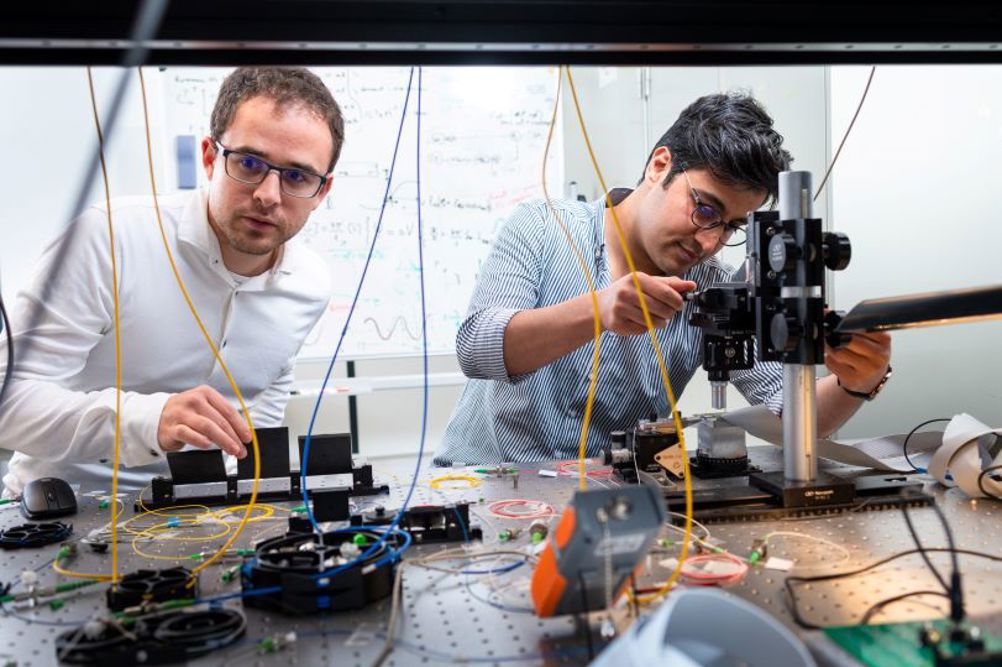
Mona Peyvasteh, PhD, whose educational background is in photonics and who now works on optics design for displays and previously worked for AR/VR firm Varjo, strongly agrees. She stresses that engineers in photonics and electronics, along with optics engineers and software developers, often have to work closely to achieve the desired results in product development.
“Designing optics for consumer electronics – screens and VR headsets, for example – requires consideration of complex factors,” says Peyvasteh.
“Photonics, electronics and software engineers contribute from an early stage of development, including concept generation or technology selection, to the last stages of manufacturing and production. In the design and development phase, we need to define the overall system architecture, including the interaction between optical, electronic, and software components, and ensure smooth integration of optical components with electronics and software. You can find these kinds of close collaboration between optics and photonics in different applications including AR/VR devices, wearable medical devices (biosensors), and automotive displays,” she adds.
Testing: no light work
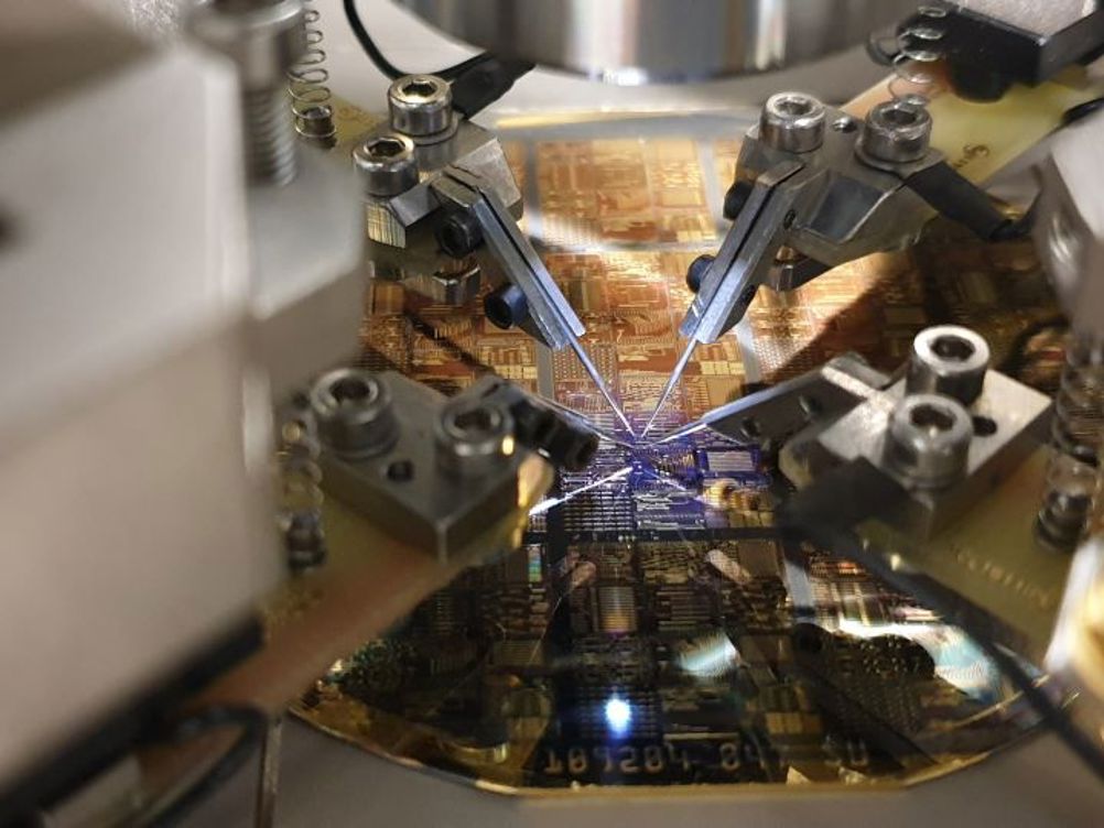
While promising in scope and trajectory, the field of photonics does face significant challenges related to testing and development. “Testing photonic components requires longdistance transmissions with extreme accuracy, using highprecision, high-frequency lasers,” says Virte. “One problem with this is that high-precision lasers are not only difficult to make, but lasers in general are also very noisy. So far, only a small number of companies and people have really concentrated on creating precision, low-noise lasers.”
Dr Martijn Heck, a professor in the Photonic Integration Group of the Electrical Engineering department at Eindhoven University of Technology, is one of those people. Now focused on photonic integration (the process of combining multiple photonic components onto a single chip or module), Heck and his colleagues are working to develop devices that operate at microwave and terahertz frequencies and support quantum-based applications.
“There is a sliding scale for testing photonics applications,” Heck explains. “On one end, you have very complex photonic chips with 10,000 components integrated. On the other, you have simple components like LEDs. LEDs are very inexpensive and are similar to single transistors or capacitors in terms of testing and qualification.
“For telecom lasers, which are essentially laser diodes, the testing involves characterizing the optical output power. While these are electronic components, the testing is more about the light they emit rather than just their electrical behavior. These components must be tested for lifetime and performance at elevated temperatures, similar to electronics,” he continues.
“As you move to more complex devices like modulators, which are also diodes, you need both an optical input and output. Testing these requires optical and electrical probes, complicating the process because the alignment for optical probes needs to be within a micrometer, whereas electrical pads allow for a 10-micrometer margin. This increased accuracy slows down the testing process. Additionally, the types of tests required become more complex, as you need to scan not just current and voltage but also other parameters,” Heck adds.
In short, photonics and electronics require similar types of testing processes, but photons and electrons present different challenges. In both cases, signal processing outputs are evaluated and analyzed, but photonics involves a much higher level of precision.
Heck also emphasizes cost as a challenge associated with more complex testing. “For high-speed communication photonic chips, you need test equipment capable of handling high speeds and bandwidths, which is very expensive,” he says. “Standard test equipment like a one-megahertz oscilloscope won’t suffice for testing 100 gigabit-per-second components. Finally, testing photonic modules involves not just the photonic chip but also the electronic chip that drives it. This includes testing the integration of both chips, their packaging, and ensuring lifetime of the module.”
For VUB’s Virte, many of these challenges come down largely to the fact that photonics testing is only in its infancy. Equipment and techniques are still evolving, and the range of products and services around testing is therefore an expensive and dynamic area to navigate. “In terms of understanding and reliability, we are getting closer to electronics-level testing,” he says, “but we often face different problems with very different benchmarks. To progress in this area, I believe we need to collaborate more deeply with our counterparts in electronics to better understand and adapt certain models to our own work.”
A human element
In recent years, the fast pace of technological advancement has contributed to widening skills gaps in numerous industries that rely on technical expertise. Put another way, emerging tech is creating demand for new skills more quickly than people can be trained to acquire and master them. Neither electronics nor photonics is exempt from this trend, but photonics has been hit especially hard.
According to Peyvasteh: “It’s still not that common to see ‘photonics expert’ in a job posting or description. The recognition and demand for those specific skills is definitely growing, but it continues to be a relatively small field of study and practice, especially when it comes to integrating photonics in the broader scheme of devices and systems.”
This bottleneck is all too familiar to Heck: “Technical talent is always hard to get. It’s not so difficult to find PhD-level expertise, but it’s very challenging to find people with industry knowledge, or who, for example, have design experience and knowledge of testing standards. These factors make testing very hard to do at scale. Our students, for example, are very capable of testing one extremely complex chip, but they would not have the resources to test a million very simple chips.”
Virte calls it a “big discussion” among photonics companies and professionals, especially in Europe. “Scaling up development requires customers and funding, so we need to bridge the gap between research and industry to make large-scale development a reality,” he comments.
The problem led one of Heck’s colleagues, Dr Sylwester Latkowski, to help found the Photonic Integration Technology Center (PITC) in Eindhoven. PITC is a joint innovation center with an overall aim to create a funnel of integrated photonics applications that can lead to large-scale adoption. The center’s approach is based on providing shared access to training, education, tools, equipment, facilities, and analysis, helping to mitigate the high costs and technical barriers associated with photonics R&D.
Fab, fabless, foundry
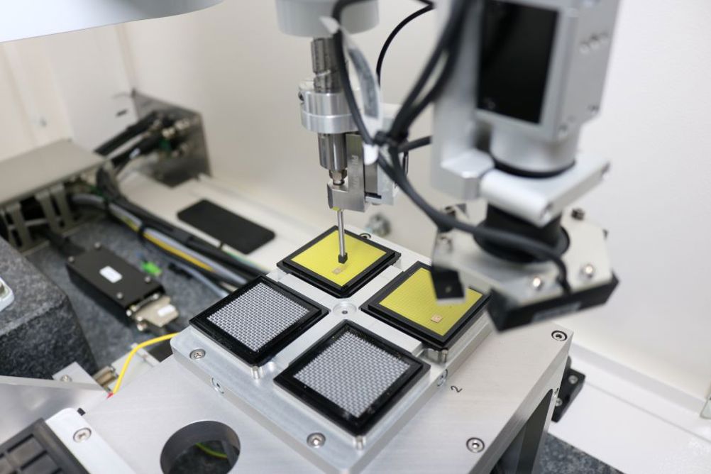
While consortia and innovation hubs like PITC represent the best of many advances in photonics testing, most facilities and business models conform to a more conventional mold. The semiconductor industry is traditionally divided into three types of companies: those that design and manufacture their chips in-house (integrated device manufacturers), those that design chips but outsource manufacturing (fabless companies), and those that focus solely on manufacturing chips for others (foundries). Photonics follows a similar pattern, though it faces unique challenges.
Integrated photonics companies are involved in both the design and manufacture of photonic components. These companies often operate on the frontiers of what is technologically possible, developing highly specialized products that make the most of their integrated approach.
Fabless photonics companies, on the other hand, focus on the design and development of photonic components while outsourcing manufacturing to foundries, a model that allows them to concentrate resources on innovation and design, leveraging the advanced fabrication capabilities of specialized foundries. Meanwhile, photonics foundries are dedicated facilities that strictly manufacture photonic components. They operate and maintain cutting-edge equipment capable of producing the highly precise and often miniaturized components required for photonics applications.
“Miniaturization is a crucial aspect of photonics design and integration,” Peyvasteh points out. “It requires precise manufacturing of small light sources, waveguides, and other optical elements that are critical for robust and reliable performance,” she says.
The challenges are substantial: producing these highprecision devices and elements requires extreme cleanliness and precision, often exceeding the standards of traditional semiconductor fabrication. But, according to Peyvasteh: “The effort is well worth it.”
Along with research institutions, design houses, and OSAT (outsourced semiconductor assembly and test) companies, these organizations and their various resources and limitations inform a complex photonics ecosystem – an ecosystem on which the future of consumer electronics may thrive.
This article first appeared in the September/October 2024 issue of Consumer Electronics Test & Development magazine. To read the full issue, click here.