
Ever since microLED display technology emerged around 2010, manufacturers, analysts, and industry experts have been excited by its potential for superior performance.
It’s easy to see why, “MicroLEDs have outstanding performance attributes. They offer higher pixel density, lower power consumption, faster (nanosecond) response time, and wider viewing angles than LED-backlit liquid crystal displays (LCDs) or organic LED (OLED) displays. Importantly, they offer an order-of-magnitude higher luminance than OLED displays or LCD in direct sunlight conditions, which is crucial for handheld devices, as well as a key enabler for near-eye displays.”1
However, establishing cost-effect fabrication processes for microLED displays has proven to be challenging, and manufacturers are still working to close the gap between promise and market reality. These nano-scale elements require multiple steps to produce, with defects potentially emerging at each step. And, as we know, the consumer device marketplace expects near-perfect visual quality and performance from today’s display devices.
To meet these high expectations, manufacturers must perform careful inspection at each step, yet also must achieve high yields to ensure production costs remain viable for the mass market. The timeline for moving microLED displays from research labs to mass production has been slow, and we’re still not quite there yet. But recent developments and advancements have helped to move the industry closer to finally achieving consumer marketability for microLED devices.
End-to-end microLED fabrication challenges
Creating microLED displays is a multi-phase process that includes some or all of the following: epitaxial growth, photolithography, chip fabrication/wafer fabrication, substrate removal, mass transfer, bonding and interconnection with the control circuit, testing, repair, panel assembly, etc.
While LED technology has been around for decades and widely used for LCD displays, microLEDs require new processes and techniques. Almost every step in the fabrication process has had to be re-invented and every component needs to be optimized for performance and cost.
For example, “Tiny micro-LEDs have a large relative surface area, which may lead to more defects during the fabrication process. Therefore, solving engineering/manufacturing challenges is important, including die size miniaturization while maintaining high efficiency, chip design, and chip manufacturing technique improvement.”2
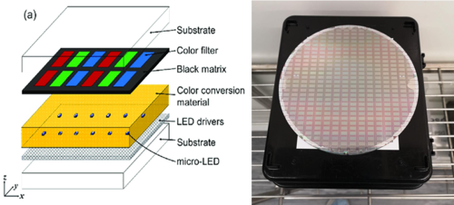
Figure one: Simplified schematic of microLED display layers (left, image source via Creative Commons). Plessey 0.26 arrays bonded to CMOS backplane for monolithic microLED displays (right, image source).
Their small size (typically <50 μm and some as small as 3 μm) presents big new challenges. “Most LEDs today are fabricated on 100 mm and 150 mm sapphire wafers, though InGaN-on-silicon is gaining in popularity, especially among large silicon-based foundries. Historically, LEDs are assembled in a surface-mount technology (SMT) package, wire bonded in place and encapsulated with epoxy or silicone. The key difference with microLEDs is they are used in bare die form rather than in packages. This difference, along with much tighter design rules, makes fabrication of microLEDs a very costly endeavor.”3
Developers are working to address challenges such as color conversion, reduced external quantum efficiency (EQE), low-efficiency and low-yield in the mass transfer process, bonding methods, and improving performance of the backplane and panel.
The mass transfer step has proven particularly challenging because traditional LED pick-and-place and flip-chip methods don’t work for tiny microLEDs. Methods such elastomer stamp, laser-induced transfer, fluidic self-assembly (FSA), roll-to-roll (R2R) or roll-to-panel (R2P) transfer, electrostatic transfer, and more have all been tried with mixed success.4
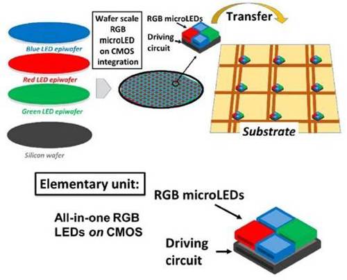
Figure two: One fabrication method for microLED displays uses integrated CMOS driving to simplify the transfer step. The result is an elementary unit consisting of all-in-one RGB LEDs on a CMOS driving circuit. (Image source: eenews)
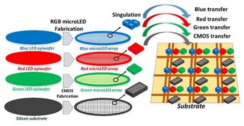
Figure 3: A more complex approach focuses on singulating blue, red, and green LEDs from their wafers as well as CMOS driving circuits to transfer each separately. (Image source: eenews)
Latest breakthroughs and advancements
Despite all these challenges, microLEDs remain a focus of research and development activity, and creative new techniques and solutions continue to emerge. Samsung’s recent announcement of a 110-inch microLED television is only the latest sign of progress. Although it is priced at a hefty US$155,000, experts anticipate economies of scale will eventually prevail in this market.5

Figure 4: Samsung’s 110-inch microLED television offers 4K resolution with 8 million pixels. (Image: Samsung, Source)
Some other recent advancements include:
- Development of a new integrated laser system for microLED manufacturing from Coherent. It performs three steps in the fabrication process: Laser Lift-Off (LLO), Laser-Induced Forward Transfer (LIFT), and Repair/Trimming. By combining these it can potentially lower manufacturing costs.
- Researchers at universities in Shanghai, Taiwan, and Chengdu have been looking at solutions for producing full color microLED displays, including new advancements in growth techniques, transfer printing, and color conversion.
- The world’s first stretchable microLED display was unveiled in 2021 by Royole. These new stretchable displays are not only foldable and rollable, but also capable of 3D freeform shaping, including pulling, twisting, convex and concave deformations.
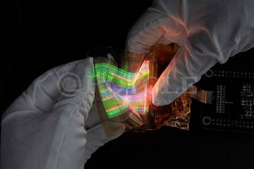
Figure 5: A flexible new microLED display is stretchable, foldable, and rollable, opening new possibilities for wearable and embedded displays. (Image: Royole)
MicroLED inspection requirements
Defects, variations in color or brightness, and other irregularities can quickly deflate buyer satisfaction, hurt brand reputation, and erode market share. Foundries and fabricators must meet near-zero tolerance for defects in finished display devices. If quality issues cannot be addressed and corrected at the component level, low yields and high production costs will impede the viability of microLED display technologies for the mass market.
Due to the complex, multi-stage process of fabricating microLED displays, quality inspection must also be conducted at multiple stages. Manufacturers don’t want to miss defects at the chip/wafer stage that could end up built into an assembled device, which then must be discarded along with all its invested parts and labor. Inspection at key points throughout the process is critical.
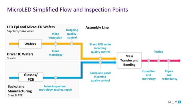
Figure 6: LED fabricators are stepping up their use of inline metrology, automated optical inspection, and testing protocols. (Image source: KLA)
MicroLED inspection solutions for every fabrication stage
Whichever microLED fabrication methods ultimately prove most successful, the need for quality assurance throughout the manufacturing process is pervasive. With nearly 30 years of experience developing solutions for all stages of electronics production, Radiant already offers a full suite of measurement and inspection solutions for microLEDs from the chip/wafer level to the panel/assembly level.
To ensure the absolute quality of microLED display devices, Radiant’s measurement solutions (including ProMetric Imaging Photometers and Colorimeters with optional Microscope Lens) are enabling microLED manufacturers to asses display performance and uniformity at multiple fabrication stages with accurate and repeatable results.
Because microLED displays are emissive (each microLED pixel is individually powered and emits its own light), variation in luminance and chromaticity from pixel to pixel can result in uniformity issues. Applying patented demura methods, Radiant’s high-resolution imaging systems and TrueTest software enable manufacturers to accurately inspect and correct each pixel and subpixel element to increase yields.
For extremely precise inspection of individual pixels and subpixels, Radiant’s ProMetric systems offer the high-resolution imaging necessary to capture and measure the discrete output of each pixel and to register subpixels correctly regardless of shape or layout. Typically applied for subpixel characterization in R&D and lab environments, Radiant’s Microscope Lens enables the full resolution of the imaging system to be applied to a very small (zoomed-in) portion of a display or wafer, for exponentially greater measurement precision at each light-emitting element (each individual microLED).
Once microLEDs are transferred to a backplane, Radiant’s measurement systems can be used to evaluate luminance and color uniformity across the entire panel at once. The advantage of a 2D imaging photometer or colorimeter is the ability to capture a large spatial area in a single image, comparing measured values to detect and qualify any areas of nonuniformity or mura (blemishes).
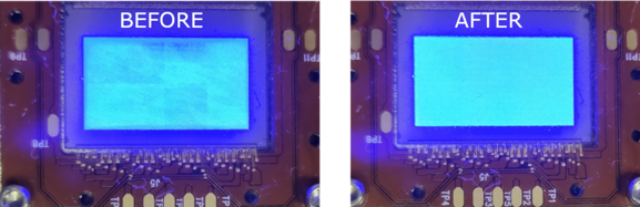
Figure 7: MicroLED from Jasper Display shown before and after uniformity correction (demura) using Radiant's solution.
Radiant’s ultra-high-resolution imaging systems (up to 61MP) can also take a single image of a display for evaluation but can further measure pixel-level luminance and color values for all pixels in the display at once, even without a microscope objective lens. These comprehensive measurements enable very efficient pixel uniformity testing and calculation of correction factors for display calibration (demura) in production settings.
To learn more about solutions for microLED quality inspection and correction, read the whitepaper: Measuring and Correcting MicroLED Display Uniformity.
References:
- Peters, L, “MicroLEDs Moving from Lab to Fab.” Semiconductor Engineering, July 22, 2021.
- “Micro-LED display development unhindered by COVID-19.” Semiconductor Today, July 16, 2021.
- Peters, L, “MicroLEDs Moving from Lab to Fab.” Semiconductor Engineering, July 22, 2021.
- Wu, Y, et al, “Full-Color Realization of Micro-LED Displays.” Nanomaterials, December 10, 2020.
- Chen, Z, Yan, S, and Danesh, C, “Topical Review MicroLED technologies and applications: characteristics, fabrication, progress, and challenges.” Journal of Physics D Applied Physics, January 2021.