
Excitement about metalens optics continues to grow, as scientists and entrepreneurs explore new methods and use cases. Developments in metamaterials and metalenses have come fast and furious in recent years.
For example, EPIC (European Photonics Industry Consortium) just held a Technology Meeting on Metamaterials and Metalenses. New research breakthroughs include:
-
MIT scientists developed a metalens that transforms incoming UVA light into a focused output of vacume UV (VUV) radiation, which can potentially reduce the complexity of semicondoctor manufacturing. Learn more...
-
A metalens design developed at Harvard University uses millions of holes (instead of the typical pillars) to focus light to a single point. Learn more...
New metalens products and components were also on display at the recent SPIE Photonics West Exhibition in San Francisco.
-
For example, NIL Technologies showed off a new metalens camera module.
-
Synopsis, Inc. presented at the conference on their fully automated inverse design solution for metalenses/metasurfaces
-
Conference attendees could attend talks about a new fisheye-metalens stereo camera from MIT or a metalens array for smart sensing developed at City University of Hong Kong.
The origin of metalenses
The concept of metamaterials has been around for a while, but the last two years has seen a surge in scientific and fabrication breakthroughs that could soon usher in a new age of optical techniques and capabilities based on metalenses.
The term “metamaterials” was coined from the Greek word meta, which means “beyond”—metamaterials go beyond normal materials in the sense that the natural properties of the materials have been altered.
Metalenses are tiny optical elements that can manipulate electromagnetic waves (light)—just like traditional lenses—but are thinner than a sheet of paper. The technology is exciting to developers across many industries due to their small size, ease and cost-efficiency to manufacture at scale, and their potential to revolutionize multiple optical applications.
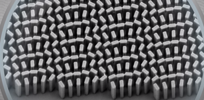
An example of possible metalens patterns, captured by electron microscope. Picture: Science Magazine video/YouTube
Shrinking technology
The history of modern technology development has been a steady progression towards miniaturization, as computer chips and other electronic components have gotten increasingly smaller. For example, all the computing power that NASA used for the 1969 moon landing was far less than what now fits in your pocket on an average cell phone.
However, until metamaterials, there had been no way to significantly shrink lenses used in cameras, microscopes, telescopes, and other optical equipment. The size of lenses has been constrained by the material properties (refractive index and dispersion) of glass—or in recent decades, plastics. In essence, we are still using a medieval tool (the glass lens) and 19th century optical technology that we’ve not been able to improve on beyond achieving greater precision in shaping and grinding.
The structure of metalenses
Traditional lenses work by bending light waves. Lenses with different thickness or varying thickness bend the waves in different ways. When a wavefront passes through the lens, light waves at different parts of the lens are refracted at different angles. Often multiple individual lenses are stacked together (called compound lenses) to direct and control light in specific ways.
In contrast to traditional lenses, the concept of a metalens is a single thin, flat structure with multiple waveguides—like tiny pillars—arranged in specific patterns. These pillars, which have been likened to antennae, are nanoelements made from titanium dioxide (TiO2) that measure approximately 600 nanometers (nm) long—shorter than the length of 10 hydrogen atoms laid side by side.
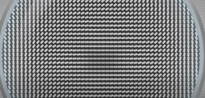
Another example of possible metalens patterns, captured by electron microscope. Picture: Science Magazine video/YouTube
Because metalenses are flat (planar) and ultra-thin, they do not produce chromatic aberrations—they are “achromatic”—because all wavelengths of light pass through virtually simultaneously. Their advantages also include tunable dispersion—the ability to manipulate how colors of light are dispersed—as opposed to glass or other tradition materials that have fixed dispersions. Additionally, metasurfaces can be mass produced in existing CMOS semiconductor foundries, enabling massively-parallel wafer-scale integration of optical systems.
Metalens breakthroughs
A significant milestone in the development of metalenses came in 2016 when researchers from Harvard University’s John A. Paulsen School of Engineering and Applied Sciences (SEAS) demonstrated the first planar lens that worked efficiently within the range of visible light, covering the entire spectrum of colors from red to blue.
Calling the waveguides “nanofins”, the SEAS team, led by Federico Capasso, designed their metalens to focus light onto a single point approximately 400 nm across. Their metalens was the first to be able to focus the entire spectrum of visible light and offered optical performance better than any current commercial lenses.
This development was followed in 2018 by an announcement of the first two-dimensional metalenses with nanostructures the same size as the wavelengths of light that pass through them, created by a team from the University of Washington and Taiwan’s National Tsing Hua University.
Soon after, a Columbia University Engineering team created the first flat lens capable of correctly focusing a large range of colors of any polarization to the same focal spot without the need for any additional elements. Only a micron thick, their flat lens uses “meta-atoms” to focus light with wavelengths ranging from 1.2 to 1.7 microns—in the invisible near-infrared range—to the same focal spot.
Following on from these breakthroughs, there was a wave of additional metalens developments —we could almost call 2019 the Year of the Metalens.
-
In January 2019, the SEAS team at Harvard announced the development of a new “polarization-insensitive metalens comprising non-symmetric nanofins that can achromatically focus light across the visible spectrum without aberrations.”4 Previously metalenses could only focus circular non-polarized light, effectively losing half of the incident light which did not match the polarization.
-
In May 2019, mathematicians at the Massachusetts Institute of Technology (MIT) published the results of their work to develop a computational technique that quickly determines the optimal makeup and arrangement of metalens nanoelements. This will enable makers to design metalens patterns to meet specific objectives, such as controlling colors or creating different shaped beams.
-
In July 2019, researchers at the University of Michigan announced a new technique that uses a set of metalenses to focus light into a specific pattern, rather than a single point. This approach has implications for any beam-shaping applications such as laser cutting, annealing, and selective crystallization.
-
Also in July, researchers at Saudi Arabia’s King Abdullah University of Science and Technology (KAUST), develop a method of twisting a slack of metalens films to further control the properties of light. For example, they developed a bifocal metalens with controllable focal length and intensity ratio.
Related to metalenses is the rise of wafer-level optics. Wafer-level fabrication and integration of micro-optical components is enabling the application of micro-structure technologies to camera module manufacturing. Essentially, camera lenses can be manufactured using semiconductor processes to imprint individual microlenses on wafers. Wafer-level camera modules have tight tolerances for alignment shape, thickness/uniformity, but can offer more efficient fabrication at high volume.

Display technology like digital cameras is likely to be revolutionized by the emergence of metalens technology. Picture: Pixabay
Metalens applications
Metalens technology is now poised to revolutionize cameras, displays, and other optical devices. Some of the exciting potential applications include:
-
Chip manufacture – The University of Michigan’s method for creating patterns of light can be applied by chip manufacturers who use light to carve specific patterns onto the surface of a silicon slab. Using metalenses will potentially enable more complex patterns to be produced more efficiently and with a low rate of defects.
-
AR/VR/MR – developers of XR systems continue to wrestle with the challenge of incorporating bulky hardware systems into devices to be worn on the head. Metalenses offer the prospect of tiny optical elements incorporated into small, high-performing, lightweight headsets and smart glasses.
-
Medicine – the enhanced optical capabilities of metalenses can enable more precise diagnostic imaging than ever before, higher-resolution imaging tools such as endoscopes, and new microscope form factors, enabling radiologists, physicians, and lab technicians to see details that were previously invisible.
There are still challenges to overcome: “expenses are still high because it is difficult to precisely place nanoscale elements on a centimeter-scale chip…So far metalenses do not transmit light as efficiently as traditional lenses do—an important capability for such applications as full-color imaging. In addition, they are too small to capture a large quantity of light, which means that, at least for now, they are not suited to snapping high-quality photographs.”
Nevertheless, meta-technologies hold great promise for the continuing development of optical, imaging, and display systems. With Radiant’s 20+ years of experience in precision measurement of light and color and our work with optical and display systems at both full- and nano-scale, we’re excited to see what comes next.
This article originally appeared on Radiant Vision Systems website and is only reproduced here with their kind permission.