
The MADRAS project has boosted, thanks to a set of new advanced inks and substrates, the manufacturing of a battery-free localisation tag and a fingerprint detector for unlocking shared scooters, two innovative consumer electronic products.
MADRAS, an initiative funded by the European Union’s Horizon 2020 programme and coordinated by Eurecat Technology Centre, has contributed to boost the production of organic and large area electronics devices by establishing a high-speed manufacturing methodology with optimised materials with improved conductivity and transparency.
“The impact generated by MADRAS has increased the industrial competitiveness of European consumer electronics companies by providing them with a low-cost manufacturing process and improved materials’ lifetime and processability,” explains Rosa Araujo, MADRAS project coordinator and project manager at Eurecat.
The materials developed consist of a sustainable nanocellulose substrate and different types of advanced inks, including semiconducting transparent inks based on organic components, transparent conductive silver nanowires-based inks and semiconductive inks based on metal oxide nanoparticles.
Flexible electronics produced as part of the MADRAS project. Picture: Eurecat Technology Center
These inks have been implemented as transparent conductive electrodes and hole transport layers, allowing the development of devices by printing techniques with increased robustness, while reducing their cost and environmental impact.
The implementation of these materials in the manufacturing of electronic devices provide viable alternatives to conventional inorganic conductors and semiconductors, such as copper or silicon, providing the resulting product with higher device robustness, cost reduction, and a reduced environmental impact.
Conductive and transparent nanocellulose substrate
The first material developed is a substrate based on cellulose nanofibrils films made from renewable resources, mostly wood. It has been optimised up to a transparency of 90%, which is the level needed to substitute most of the current polyester films used currently.
According to Gael Depres, Central R&D Manager at Arjowiggins, the conductive and transparent paper substrate developed “offers a green alternative to replace plastic substrates in electronic devices, which are made from oil or natural gas, as its more sustainable and recyclable, even with ink tracks printed on it.”
Advanced conductive and semiconductive inks
Several transparent and conductive inks based on silver nanoparticles and silver nanowires have been developed, suitable for slot die and screen printing with enhanced properties in terms of stability, transmittance, conductivity and adhesion.
Additionally, inorganic semiconductive nanoinks based on tungsten oxide have been created to enhance the charge mobility and conductivity of the hole transport layer in photodetector electronic devices.
These types of inks represent a step further in the replacement of indium tin oxide as the transparent conducting material used in most transparent conductive electrode applications. While indium tin oxide has outstanding conductivity and transparency properties, it is a scarce material and shows limited flexibility, requiring a heavy vacuum method for deposition.
Benjamin Dhuiege, Head of R&D at GenesInk, highlights the sustainability of these inks, ensuring that they are “easy to process, without any toxic component and with high-added value through customisation.”
MADRAS has also performed research on inks based on conductive polymers. Conductive polymers are one of the most widely used organic-based materials in printed electronics, being poly(3,4-ethylenedioxythiophene) (PEDOT) the most frequent one, both in research and in practical applications.
Several transparent and conductive inks have been developed. Picture: Eurecat Technology Center
The use of organic materials suitable for functional layers of printed electronic devices “is linked to the need to optimise the material, including the composition of the printing ink formulation, to suit the given functionality,” adds Lubomir Kubac, Executive Head of the Centre for Organic Chemistry (COC).
In the MADRAS project, a PEDOT:PSS conductive polymer ink has been developed and applied either as a hole transport layer or as a transparent conductive layer in the fabrication of organic photodetectors.
PEDOT:PSS inks provide a charge carrier mobility of 0.7 cm2/V.s, allowing an effective transport of holes, and a conductivity of 500 – 900 S/cm. Their formulation has been designed and optimised using different solvents to enhance printability, layer thickness and homogeneity of the layer considering the scaling-up conditions.
“Organic-based materials offer a unique opportunity in terms of tuning their electronic properties to achieve suitable functionality in multilayer electronic structures” details Tomáš Syrový, Associate Professor at the University of Pardubice.
An innovative and scalable manufacturing methodology
The advanced materials developed within the project have been processed and upscaled through In-Mould Electronics, a manufacturing approach that allows adding intelligence and functions to plastic components. This process combines the functional printing of electronics and the hybridisation of electronic components with traditional plastic transformation processes, such as thermoforming and injection.
“In-Mould Electronics is triggering the mass production of printed electronic products embedded in plastic parts allowing customising new and traditional products in many different industries and enhancing Europe’s leadership position on organic and large area electronics,” points out Laura López, researcher at Eurecat’s Functional Printing Unit and MADRAS technical coordinator.
Consumer electronic products made of advanced materials
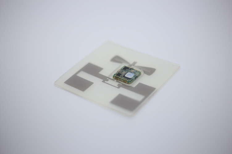
As a result, these materials and manufacturing processes are being validated in two different consumer electronic products, a geotracking flexible tag to localise assets without any battery usage thanks to far-field wireless power transmission, and a biometric photosensor which will be employed to identify users of an electric mobility service.
The tag, being deployed at UWINLOC, can be attached to tools, vehicles or parts in a logistic shopfloor for the localisation of assets at any time, helping to achieve real-time inventory and a better stock management.
Thanks to the use of sustainable inks and substrates and the in-mould electronic process, the tag development has been less complicated and costly, from the choice of the materials to the printing process, the hybridisation techniques and the integration through injection moulding for protection.
The MADRAS team has created a fingerprint reader for the shared mobility market. Picture Eurecat Technology Center
“This tag allows us to track a large volume of assets like tools or card boxes along manufacturing lines and in warehouses, helping operators spend less time looking for them when they are lost and allowing further process automation, thus improving the overall productivity,” indicates Eric Cariou, Business Developer at PARAGON ID (ex UWINLOC).
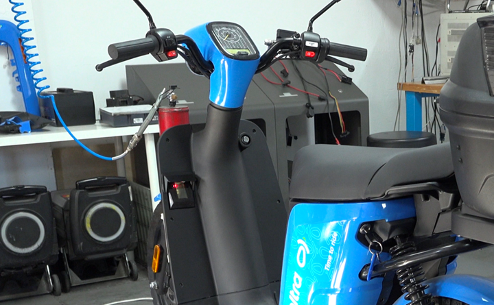
The other project innovative device to validate the unique MADRAS technology approach based on applying advanced materials and soft fabrication techniques in the development of organic and large area electronic devices, is a fingerprint reader for the shared mobility market.
Ricard Gomicia, Electric Vehicle Manager at Cooltra, indicates that this innovation can help them “ease users’ access to our scooters, since both registration and booking can be done in a single step”. Moreover, it constitutes “a solution to mitigate the usurpation or falsification of user’s identity.”
Common fingerprint readers are inorganic, mainly made of silicon rigid substrates and evaporated materials. MADRAS, on the other hand, leaps forward by developing a device with a photodetecting fully printed frontplane based on the advanced materials and in-mould electronics manufacturing processes.
The fingerprint reader is capable to scan and identify users’ fingerprints thanks to an optical imaging component, activating, through telematics and a back-end interface the shared scooters. With near-infrared photosensors, additional biometric data, such as heart rate, can be collected in order to validate that a real human is approaching the sensor.
The MADRAS project is formed by a multidisciplinary consortium made up of 12 partners from Spain (Eurecat, Eticas Research and Consulting, Tecnopackaging, UNE and Cooltra), France (Genesink, Arjowiggins and UWINLOC), Denmark (infinityPV), the Netherlands (TNO) and the Czech Republic (COC and the University of Pardubice).
This article is authored by researchers from the Functional Printing Unit at the Eurecat Technology Centre of Catalonia. To find out more about the MADRAS project click here.