
Our world is facing huge environmental challenges and solutions to replace non-eco-friendly materials. In consumer electronics, Organic and Large Area Electronics, known as OLAE, are seen as a viable alternative to conventional inorganic conductors, such as copper and silicon. Instead, OLAE works with carbon-based materials such as polymers, small molecules or innovative nanomaterials made by nanoparticles or nanowires, expanding the world of electronics in ways unimaginable until now.
The latest developments in organic electronics, printed on flexible substrates, such as plastics or paper, allow the development of more sustainable electronics devices, including the production of smart packaging, roll-up displays, flexible solar cells, single-use diagnostic devices and printed batteries along with other innovations. OLAE is an emerging technology ideal for applications that require flexibility and adaptability to large areas, proposing cheaper, less toxic, and more sustainable solutions.
Despite all the advantages that OLAE presents, ranging from the possibility to develop ultra-lightweight devices to a low-cost fabrication of printed electronics, the technology presents multiple technological hurdles. Open challenges include the lack of manufacturing processes’ stability and processability, and the need for scalable production methodologies for OLAE mass production, in addition to the need for materials with improved properties, its synthesis and novel routes for its encapsulation.
The goals of the MADRAS project
The European MADRAS project, funded by the European Union’s Horizon 2020 programme and coordinated by Eurecat Technology Centre, aims at boosting the production of OLAE devices by establishing a high-speed manufacturing methodology using optimized materials with improved conductivity, charge mobility and transparency.
MADRAS innovation bring to the electronics market more affordable and durable OLAE-based products for high-volume production by developing advanced materials to be promptly processed via In-Mould Electronics (IME), merging two different manufacturing processes – printed electronics and plastic processing based on injection moulding and thermoforming. This will allow the creation of a new generation of plastronic products with enhanced properties. MADRAS results will be applicable to a wide range of industries, such as the Internet of Things, automotive, healthcare, logistics, packaging and the wearables’ sector.
In the words of Laura López, researcher at Eurecat’s Functional Printing Unit and MADRAS technical coordinator, the MADRAS project aims to “demonstrate an improvement in OLAE devices by developingsolution-based functional materials, including the appropriate selection of high-performing photoactive layers and the application of MADRAS’ customized charge selective layers, conducting electrodes and substrates that can withstand plastic processing.”
The project, formed by 11 other partners from Spain (Eticas Research and Consulting, TECNOPACKAGING, UNE and the Cooltra Group), France (Genesink, Arjowiggins and Uwinloc), Denmark (infinityPV), the Netherlands (TNO) and the Czech Republic (COC and University of Pardubice), is developing a radically new manufacturing methodology for high volume production of durable OLAE-based devices. The project addresses the use of conventional and established industrial manufacturing techniques and adapted processing tools to deliver this innovative technology closer to market.
“The project goal is to enable the future market deployment of flexible and wearable OLAE-based products, guaranteeing the use of industrially and environmentally sustainable materials and processes, that are attractive to the market for their advanced functionalities, robustness, durability, and safety,” says Rosa Araujo, MADRAS project coordinator and project manager at Eurecat. The approach is based on a set of new materials, which combined with the benefits brought by the IME process are the value brought by MADRAS for an OLAE wide deployment.
New materials for the consumer electronics market
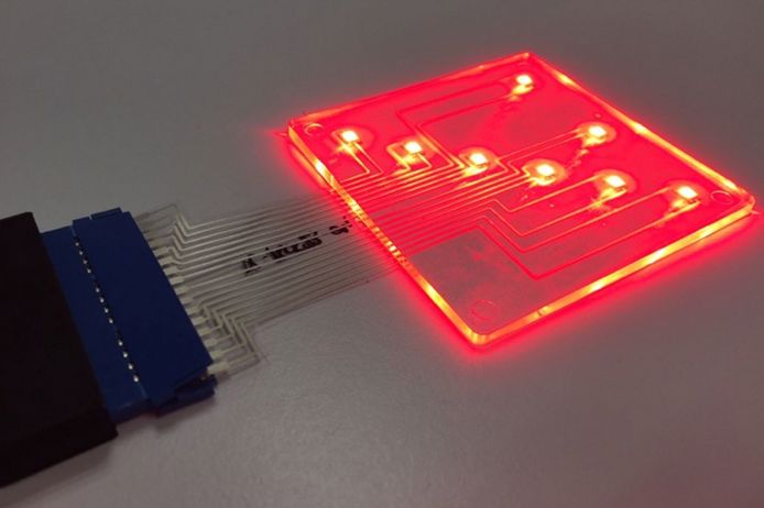
The set of new materials developed through MADRAS includes paper-based substrates and conductive and semi-conductive materials to be used as inks, with improved electrical conductivity, charge mobility and optical (transparency) properties, compared to common OLAE materials. Current Transparent Conductive Electrodes (TCE) for optoelectronic devices lack flexibility due to the use of non-flexible, expensive and scarce materials such as Indium Tin Oxide (ITO). Specifically, materials being developed include conductive and transparent substrate based on nanocellulose foils and silver nanowires-based inks, highly-conductive inks based on silver nanoparticles or PEDOT:PSS, semiconducting inks either based on PEDOT:PSS or on metal oxide WO3 nanoparticles.
“These materials allow the development of devices by printing techniques with increased robustness, while reducing their cost and environmental impact, and greater flexibility, transparency and conductivity,” explains Benjamin Dhuiège, head of R&D at Genesink.
Within the project, the research on materials has focused on the development of silver nanowires inks (Ag NWs) adapted to various printing processes - slot die and screen printing - for Transparent Conductive Electrodes (TCE) applications with improved properties and exhibiting low electrical resistivity while keeping the viscosity suitable for various deposition processes. “We aim to enhance Ag NW adhesion to cellulosic and polymer substrates with up to 90 percent transmittance and achieving performances up to 10 percent higher than the ITO standard,” says Dhuiège.
A new range of nanoparticles
MADRAS is developing a new range of nanoparticles based on this material, a safe and environmentally-friendly metal oxide, doped with conductive polymers to enhance their mobility and their charge transfer properties when embedded in electronic devices. MADRAS tungsten oxide (WO3) based inks developed by Genesink, mainly dedicated to Hole Transport Layer (HTL) applications, have shown promising results in terms of mobility and charge transfer properties.
Another developed material being applied as an HTL or as Transparent Conductive Electrodes (TCE) in the fabrication of OPDs has been the poly(3,4-ethylenedioxythiophene), the PEDOT:PSS conductive polymer. “The MADRAS project is targeting a high charge carrier mobility of 0.7 cm2/V.s, which would allow an effective transport of holes from the PAL and a high conductive PEDOT:PSS inks with a target value of 500 – 900 S/cm, especially intended for transparent conductive layers,” says Tomas Syrovy, associate professor at the University of Pardubice.
During the project “we are trying to optimize the work function of the PEDOT:PSS layer and optimise it in the context of energy levels either by ink formulation composition, modifying PEDOT:PSS complex ratio or by using special kind of additives,” he adds.
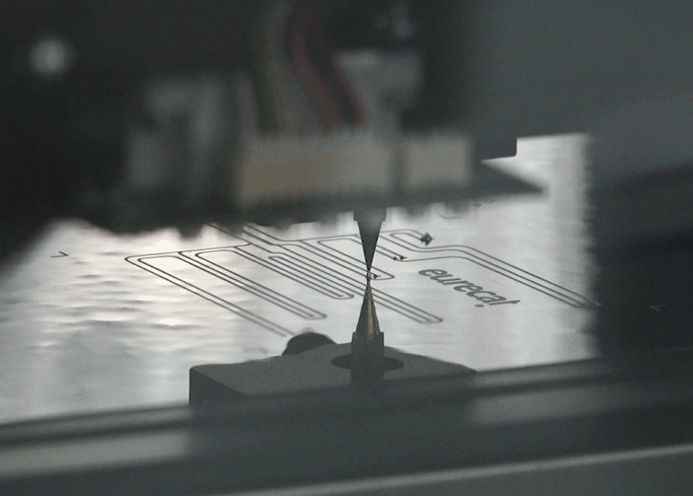
Throughout an iterative development methodology, the best ink formulation parameters have been identified to obtain the desired performance in terms of wetting behavior as well as thin film uniformity and functionality. The materials chosen are now being tested for the production of a new generation of consumer electronics market products.
Combining electronics’ functional printing and components’ hybridisation
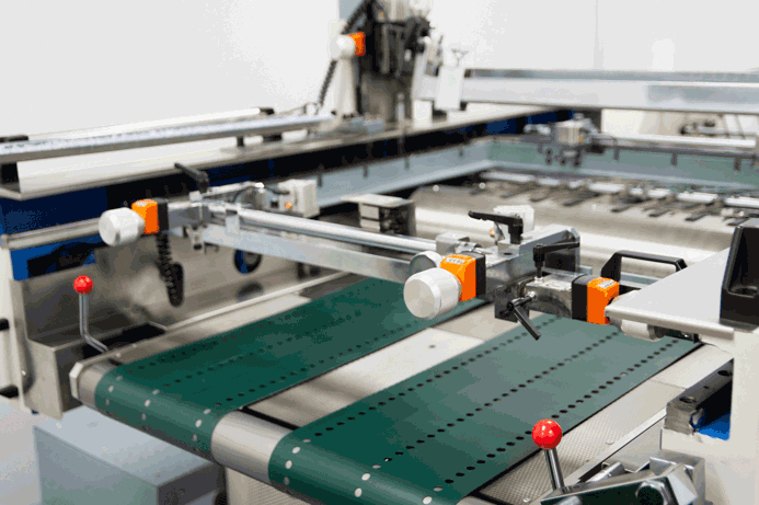
The MADRAS project will use In-Mould Electronics (IME), also known as plastronics, to enhance the device integration process, increasing resistance to humidity and wear and tear, and adding custom-made connectors. IME will be validated for the advanced materials with better conductive and resistant properties proposed in the project.
This technology allows to create plastronic products combining electronics’ functional printing and electronic components’ hybridisation with traditional plastic transformation processes, such as thermoforming and injection moulding.
IME brings a wide variety of advantages in comparison to traditional manufacturing processes, like increased functionality or more durable electronics, as active components are embedded and protected. It also eases automation, as those conventional processes are replaced with a single part that does not require further assembly after production. Additionally, the complexity of plastic products is reduced, thickness and weight are lowered, and electronics are integrated into products that have geometrically complex 3D shapes.
As part of the project, MADRAS will use Eurecat’s Plastronics Pilot Plant facilities to scale up research in new materials and processes in the IME field, a very convenient facility and starting point for the MADRAS project.
Creating a fingerprint sensor and geotracking tag
The innovative technology developed as part of the project will be implemented in two printed electronics demonstrators integrated into plastic parts, including “an in-moulded fingerprint sensor with a fully printed organic photodetector’s frontplane, and a geotracking flexible tag for the logistics sector so as to contribute to the sustainable deployment of smart products for consumer use,” notes Laura López. These products “belong to the emerging global trend of structural electronics with very large addressable markets, such as the automotive industry, healthcare and many others.”
The geotracking flexible tag will be attached to objects such as tools, vehicles and parts in assembly lines compatible with curved surfaces for their geolocalisation in company’s facilities. The fingerprint biometric readers will be integrated into scooters from a shared vehicles company aiming to increase user security and decrease vandalism. For the improvement of the users’ authentication, the fingerprint reader will include an additional heart rate sensing functionality by using NIR organic photodetectors.
The two demonstrators reflect not only large market potential applications of flexible and wearable electronics, but also demonstrate the unique MADRAS technology approach based on applying advanced materials and soft fabrication techniques in the development of OLAE devices. These real-life use cases will also show a step forward towards digitisation and IoT for its contribution to the sustainable deployment of smart OLAE products for consumer use.
This article was authored by researchers from the Functional Printing Unit at the Eurecat Technology Centre of Catalonia. To find out more about the MADRAS project click here.